LPDDR5 内存接口的高效验证和调试
5G 即将到来 – 您的测试软件能跟上时代吗?
关于 5G,我们还有很多不知道的地方。但是我们知道它速度快,它将以更高的分辨率,增强/虚拟现实和增强的游戏体验将现有的智能手机提升到一个新的水平。与 LPDDR4 相比,LPDDR5 DRAM 显著提高了数据传输速度和电源效率,满足了 5G 规范。更高的数据传输速率和更快的信号速度意味着更加复杂的设计,这些设计突破了信号完整性的界限,并需要进行更高的性能测量以进行合规性、调试和验证。
泰克 LPDDR5 发射机解决方案是一种自动化的系统级测试应用,可让您快速、有效和可靠地验证和调试 LPDDR5 设计,以满足 JEDEC 定义的 50 多种电气和时序测量要求。

加快上市时间
虽然 DRAM 验证是产品开发中确保设计质量必不可少的步骤,但它也非常耗时且麻烦。应对这一挑战的一种方法是尽可能减少手动测试。我们的 LPDDR5 发射机解决方案可以助您自动完成 LPDDR5 信号完整性测试,并将总测试时间缩短一半。这减少了总体反馈和测试周期,并可以帮助公司更快地将产品推向市场。
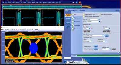
进行调试和验证
泰克的 LPDDR5 发射机解决方案将控制权归还给用户。用户自定义采集模式可让您通过自定义示波器设置(例如采样率、记录长度、带宽等)来运行 LPDDR5 JEDEC 一致性测量。
读/写突发分离一直是存储器验证工程师的主要问题。通常,在系统级别上,无法控制 DDR 总线上的数据流量。LPDDR5 发射机解决方案采用新的改进突发分离算法,不仅可以同时进行读/写突发检测,而且还可以缩短测试时间和提高准确性。
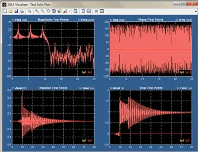
SDLA
在反嵌 LPDDR5 设计时,验证 S 参数通常是主要的考虑因素。借助改进的无源检查、端口分配和绘图功能,串行数据链路分析 (SDLA) 不仅增强了 S 参数文件的验证能力,而且还提高了灵活性,节省了时间并增加了对反嵌过程的信心。其他调试软件工具需要您完成整个过程才能找到结果。泰克的 LPDDR5 发射机解决方案可帮助您在早期阶段发现问题,从而提高调试效率并优化设计。SDLA 功能也可用于 DFE 分析。
有关更多信息,请在此查看我们的 SDLA 应用程序注释。
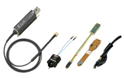
P7700 系列 TriMode 探头
LPDDR5 DRAM 的其中一种省电功能是在 1600 Mbps 或更低的数据速率运行时将三个差分信号 CK、WCK 和 RDQS 更改为单端信号。根据使用情况,还需要对单端模式以及默认的差分模式进行全面测试。带有新同轴探头的 P7700 系列 TriMode 探头端部使您可以通过一种探头设置测量差分和单端信号,而无需拆焊探讨。这简化了用于测试 LPDDR5 DRAM 单端模式的探测设置。
LPDDR5 电气验证和调试技术资料
The DDR (Dual Data Rate) is a dominant and fast-growing memory technology. It offers high data transfer rates required for virtually computing applications, from consumer products to the most powerful servers. The high speed of these signals requires high-performance measurement tools. The Tektronix TekExpress DDR Tx is an automated test application used to validate and debug the LPDDR5 designs of the DUT as per the JEDEC specifications. The solution enables you to achieve new levels of productivity, efficiency, and measurement reliability.
Key features
- Supports 52 measurements of LPDDR5 System Transmitter Tests as per DDR5 JEDEC specification:
- 09 Clock measurements
- 11 Write Clock measurements
- 11 Write Data measurements
- 07 Read Data measurements
- 07 CA Rx Specification measurements
- 07 CS Rx Specification measurements
- User-Defined Acquisition (UDA) mode for Clock, Write Clock, CA, CS, Data Strobe, and data for both Write and Read traffic (or bursts).
UDA: The TekExpress DDR Tx ‘LPDDR5’ Transmitter Solution puts control back where it should be, with the user. User defined acquisition mode allows you to run LPDDR5 JEDEC compliance measurements by customizing scope settings like sample rate, record length, bandwidth, and more
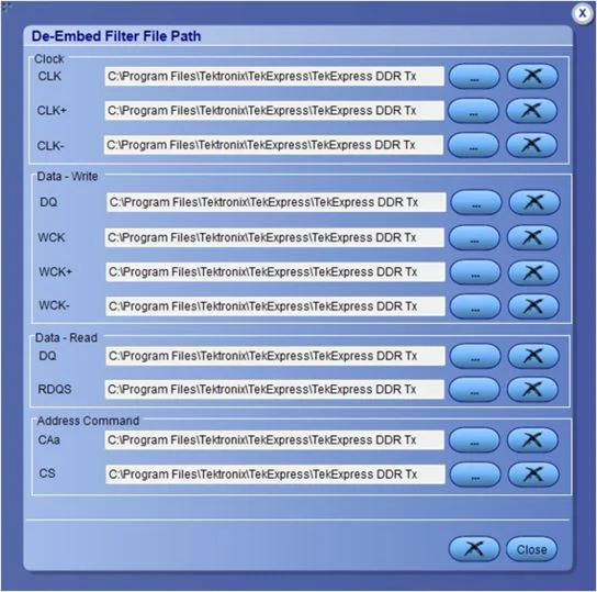
- De-embedding support for Clock, Write Clock, CA, CS, Data Strobe, and data for both Write and Read traffic (or bursts)
- Number of UIs support for Clock, Write Clock and Read/Write data measurements
- Multi-Run feature is applicable for all tests
- Save worst case waveform in known/TekExpress sessions
- Retain Vertical Scale support during acquisition
- User-friendly measurementconfigurations
- Test report to reflect all the statistics of the measurement
- User can select the source and the channel in the acquisition panel
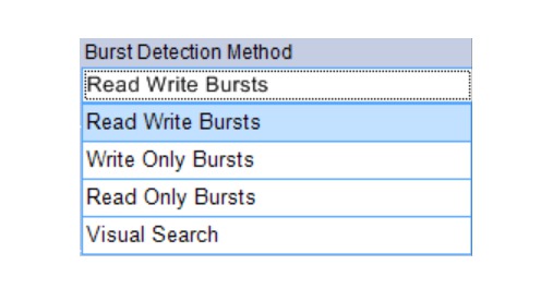
- Multiple Burst Detection Method supported - Read and Write, Write Only, Read Only, and Visual Search
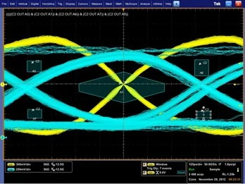
- Hexagon shape mask and margin analysis for Write Data, CA, CS Eye measurement
Applications
Tektronix provides the most comprehensive solution to serve the needs of the engineers designing DDR silicon for server, computer, graphics systems, mobile, embedded systems, and for those who are validating the physical-layer compliance of DDR Memory Compliance Test Specification.
The Tektronix option LPDDR5SYS (TekExpress DDR Tx) includes compliance and debug solution for the following:
- DRAM components
- System boards
- Embedded systems
- Mobile
- Automotive
- Internet of things (IoT)
The Tektronix option LPDDR5SYS is compatible with the following Tektronix oscilloscope models:
- DPO71604SX, DPO72304SX, DPO73304SX
- Non-ATI channels of DPS75004SX, DPS75904SX, DPS77004SX
- MSO72304DX, MSO72504DX, MSO73304DX, DPO72304DX, DPO72504DX, DPO73304DX
The above-mentioned Tektronix oscilloscopes are designed to meet the challenges of the next generation memory standards and provide the industry’s leading vertical noise performance with the highest number of effective bits (ENOB) and flattest frequency response for oscilloscopes in their class.
LPDDR5 system level tests
The Tektronix TekExpress DDR Tx solution reduces the effort and accelerates the compliance testing for DDR systems and devices with several unique and innovative capabilities.
The TekExpress DDR Tx application provides a simple, step-by-step, and easy-to-use interface to speed up the testing process. User can select the memory technology of interest in Device, Data Rate, Burst Detection Method, select the probing configuration used for Clock, and strobe in the Setup DUT panel. Perform the test selection in the next step as per the measurement group (Clock, Command Address, Data Strobe, and Data for both Read and Write traffic (or bursts)) and individual measurements within the group provide different methods of Burst detection.
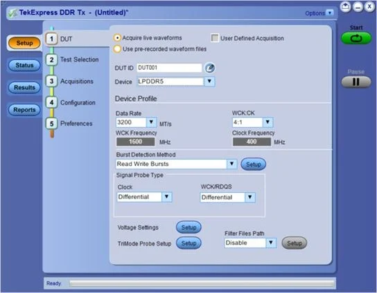
Acquisitions
The TekExpress DDR Tx application comes with a unique feature to select or deselect the signal. Once the signal is selected in the acquisition panel, the user can select the signal source connected to the oscilloscope.

De-embed filters
Easily de-embed the interposer and the probe effects by applying suitable de-embed filters within the LPDDR5 standard.
Comprehensive measurements
The option LPDDR5SYS adds a long list of JEDEC specific measurements for LPDDR5 memory standards. The TekExpress DDR Tx application covers Electrical measurements, Timing measurements, and Eye Diagram measurements as per the JEDEC standards.
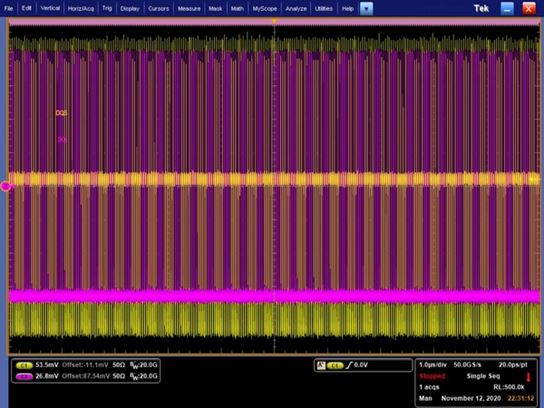
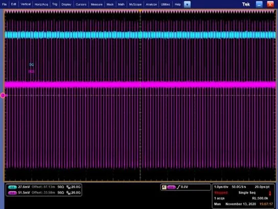
Automated Read and Write Burst detection
The TekExpress DDR Tx provides different ways to detect the burst cycles that are used to perform measurements:
- Read Write Bursts – when the DUT traffic is configured to send both Read and Write bursts then this method is used for burst detection.
- Write Only – when the DUT traffic is configured to send all Write Bursts then this method is used for burst detection.
- Read Only – when the DUT traffic is configured to send all Read Bursts then this method is used for burst detection.
- Visual Search – defining Visual Trigger areas to identify and gate area of interest for measurements
Test selection
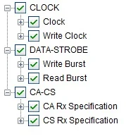
The TekExpress DDR Tx test selection panel allows the user to select the various measurements supported by the application.
- Supports 52 measurements of LPDDR5 System Transmitter Tests as per LPDDR5 JEDEC specification:
- 09 Clock measurements.
- 11 Write Clock measurements.
- 11 Write Data measurements.
- 07 Read Data measurements
- 07 CA Rx Specification measurements.
- 07 CS Rx Specification measurements.
Configurations
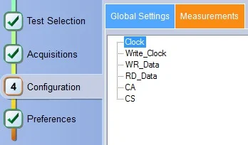
Ease of use measurement configuration to configure measurements by group instead of running through all the 50+ measurements.
Results and reporting with waveform
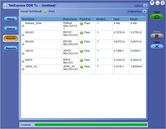
The measurement configurations and JEDEC pass/fail limits are automatically applied for the selected measurements based on the memory specification and the selected speed grade. The results report includes DDR measurements of statistical data, measurement plots, and the screenshot of the waveforms with the cursors. Hyperlinks within the report allow you to navigate between the sections.
When test execution is complete, the application automatically opens the Results panel and displays the summary of test results.

Verification versus debug
The TekExpress DDR Tx application provides a comprehensive set of JEDEC timing and electrical measurements for the LPDDR5 standard. Also, it provides access to the DPOJET Advanced Jitter and Timing analysis engine that allows flexibility to reconfigure the existing measurements or to perform new measurements that are not defined by the JEDEC specification using new user-specified test limits.
Oscilloscope triggering and waveform identification
The Tektronix Pinpoint® trigger system provides the most comprehensive high-performance trigger system in the industry. The Pinpoint trigger system encompasses threshold and timing related triggers, Dual A and B Event Triggering, Logic Qualification, Window Triggering, and Reset Triggering.
The Advanced Search and Mark feature in the Tektronix MSO/ DPO5000, DPO7000, and MSO/DPO70000 Series oscilloscopes find unique events in the waveforms. It scans acquired waveform data for multiple occurrences of an event and marks each occurrence.
The Search and Mark feature has a close relationship with the Pinpoint trigger system since they both can be used to discriminate signal characteristics. Search and Mark includes signal-shape discrimination features of the Pinpoint trigger system and extends them across live channels, stored data, and math waveforms.
The Visual Trigger makes the identification of the desired waveform events quick and easy by scanning all the acquired analog waveforms and comparing them with the geometric shapes on the display. By discarding the acquired waveforms which do not meet the graphical definition, Visual Triggering extends the oscilloscope’s trigger capabilities beyond the traditional hardware trigger system.
Supported oscilloscopes
DPO71604SX, DPO72304SX, DPO73304SX, DPS75004SX, DPS75904SX, DPS77004SX, MSO72304DX, MSO72504DX, MSO73304DX, DPO72304DX, DPO72504DX, and DPO73304DX.
Recommended probes
| Active probes | Description |
|---|---|
| P7720 | 20 GHz TriMode probe with TekFlex connector technology |
| P7716 | 16 GHz TriMode probe with TekFlex connector technology |
| Probe tips | Description |
|---|---|
| P77STFLXA/P77STCABL | Active, Solder-in Tip with TekFlex connector technology, probe tips to probe directly on the motherboard/vias or interposers with 0 Ω resistor. |
| P77STFLXB/P77STLRCB | Active, Solder-in Tip with TekFlex connector technology, probe tips to probe on the SI Interposer with 100 Ω resistor (Nexus XH Series Interposer). |
| SI Interposer | EdgeProbeTM, Direct Attach, and Socketed Interposer are available from Nexus. Order directly from Nexus. Request the s-par files for all individual signals on the interposer instead of getting a generic nominal s-par model.
Refer the Nexus's page for more information:http://www.nexustechnology.com/products/memory-interposers/lpddr5-mobile-memory-interposers/ |
